 Documentations
- ARRL review in PDF Technical manual in 4 parts 1 2 3 4
- TS850 connectors pinout
- IF232 instruction manual in PDF (1 Mb)
- All KENWOOD connectors
- Hidden menus
Modifications
- Separate receiver input
- CW monitor level
- High speed CW modification
- Audio attenuator for the DRU-2
- Additionnal CW keying input
- Better low band sensitivity
- Noise blanker improvement
Repairing
- No RX in CW/SSB but OK en FM
- Mixer FET replacement
- Clicks with "NOTCH ON"
- Low or no reception
- Modulation distorded with TNC connected
- Power level adjustement
- ALC problem on TS850 (DC-DC board)
- Gas discharge tube DSA301LA replacement
- Replacement of the CARRIER board by IW3AUT
Addons
Links to other TS850 pages
- Kenwood bulletins FTP site
- The TS850 repair page repairing the TS850
- DK9IP's page mods and manuals
- K0BX's page a lot of infos and links
- EB5AGV's page repair with high res. pictures
- IW3AUT's page who has developped very nice boards for replacement of the CARRIER board and a TCXO !
- RF SYSTEM who is selling replacement parts adn mainly the CARRIER board by IW3AUT
SEPARATE ANTENNA INPUT FOR THE TS850S
One major drawback of the original TS850s is the lack of a separate input for a receiving antenna. The first thing i did on mine was to repair this. As i had the transceiver opened, i also modified the DRV output used for a transverter. Here is how to do that.
Remove top and bottom covers, RF unit shield, RF filter shield, rear panel after unsoldering the SO239 antenna connector.
Drill 2 holes which will support 2 CINCH connectors labeled RX ANT, RX IN. You should drill these holes about 16mm under the upper connector raw (ACC1, ACC3, DSP) on the rear of the TS850S.
Remove the small board on which the SO239 is soldered on the upper part of the transceiver, cut the trace and solder 2 small coax cables as shown on figure 2. The other ends of the cables are soldered on the RX ANT and RX IN CINCH.
If you want to add a TRANSVERTER TX output which is safer than the original one which needs a 12V to be activated, follow the below instructions.
Drill 2 more holes which will support 2 more CINCH connectors labeled DRV OUT, PA IN. Remove the small coaxial cable plugged in CN2 on RF unit, unsolder the RF connector which will be used later and solder this end to the PA IN cinch.
Solder the small connector recuperated on the end of a small coax cable, plug this end in CN2 on the RF unit, the other end of the cables will be soldered on the DRV OUT cinch.
Check all again. Are the labels on the CINCH connectors correct ? Are the cables at the right place ?
Reassemble all the boards and shields, don't forget to solder the SO239 connector.
Small pieces of coax cable with CINCH males will connect the RX ANT and RX IN, DRV OUT and PA IN respectively.
Now you can use a separate RX antenna, connect an RX filter between antenna and RX, connect a transverter without the risk of burning it due to too high TX output. The output level i measured, varies from 10 to 14 dBm, depending of the operating band.
That's it !! But PROCEED at YOUR OWN RISK !!
 |
 |
 |
| Fig 1 The CINCH connectors (21Kb) |
Fig 2
Platine de commutation antenne (62Kb)
|
Fig 3 Connexions sur RF unit (59Kb) |
CW MONITOR MODIFICATION on the TS850s
(by SM4OTI via packet and from BCC handbook)
Another drawback of the TS850s is that the CW monitor level cannot by modified with the MONI pot on the front panel. Here is how to do it.
Originally the CW level is controlled by VR5 internally and has to be at a fixed level. Using headphones or the loudspeaker makes a big difference, so this modification allows to adjust the CW sidetone with the MONI pot. like for SSB.
1) Remove the IF-UNIT (you must solder on the rear side of the IF-UNIT). Be carefull to mark all the cables before you remove them!!!
2) Remove R239 (330 kohm, close to VR5).
3) Install a new resistor (330 kohm) and a 0.1uF capacitor as described below.
4) Adjust VR5 to maximum audio level.
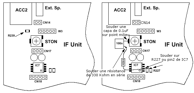
Drawing from BCC Handbook
Now you're able to adjust your audio level in the CW mode with the "MONI-knob" at the frontpanel of your transeiver.
That's IT !! But again, PROCEED at YOUR OWN RISK !!
BETTER RX SENSITIVITY ON 0,5 to 1,6 Mhz.
(by KA3PGN)
This mod greatly improves the sensitivity and likewise the reception on the AM broadcast band. No noticable unwanted side effects have occured following this procedure. I live within three miles of a 5,000 watt broadcast station on 1150 kc's and am able to listen to stations on either side of that station. There is some splatter but using the notch filter and the attenuation on the front of the radio takes care of that for the most part.
This is *NOT* complicated and can be done in fifteen minutes. Only one caution here: you WILL BE SOLDERING TWO POINTS ON A CIRCUIT BOARD THAT IS LOADED WITH SURFACE MOUNTED COMPONENTS!!! There is little room to work on the board, so be very careful with your iron! If you don't feel comfortable soldering, get someone else to do it as you can cause a solder bridge and ruin your radio without even trying.
With that in mind, here goes:
1) remove the eleven screws that secure the bottom cover to the rig. the six ones on the sides and the five on the bottom cover itself.
2) remove the bottom cover. there are no wires attached to the cover. lift it right off. leave the top cover of the radio ON.
3) locate the RF BOARD. it's number is: X44-3120-00. this is the board where you plug the optional filters into. with the open radio in front of you, and the front of the radio facing you, the RF BOARD is the one on the left. (there are only two boards under the bottom cover)
4) locate the chrome like shield on the rear of the RF BOARD. it's made out of shiney steel. remove the four screws that hold this shield to the board.
5) remove the shield by lifting the front of it up while sliding it forwards, towards you. watch out for all the little wires and ribbon cables going to and from the RF BOARD.
6) look at the rear of the board and towards the left corner.(the radio is stil facing you upside down) notice two I/C's numbered IC1 and IC2. directly behind the I/C's are a bank of adjustable coils in metal cans. there are nine of these coils in a group. directly to the left of these coils are many green and red inductors which are standing up. they look like resistors but they're really small coils.
7) these inductors are part of the bandpass filtering for each of the bands on the radio. the capacitors and resistors that complete the bandpass filtering are on the other side of the board and are of the surface mount type. you are only concerned with the bandpass filter for the .5 to 1.6 band. notice the numbers for the inductors. find L8 and L9. they are right at the edge of the board in the left rear corner you will notice that .5 - 1.6 is stamped right next to L9. BINGO! you have found the part of the circuit that you will modify.
8) look at where the .5 - 1.6 is stamped on the board next to L9. you will see two bronze or gold solder points there directly next to the numbers .5 - 1.6 . there is nothing soldered at those two points. this is where you will solder a jumper wire between the bronze points. do NOT confuse it with the other two solder points with the line running in between them next to the phillips head screw!!! you want the two points that are spaced very close together that is right next to L9.
9) you will have to do the soldering on the OTHER SIDE OF THE BOARD. remove the nine phillips head screws that hold the RF BOARD to the chasis.
10) on the back of the radio, look for the switch stamped SW 1. it's right below the grounding post and has the two postions: INT and EXT. remove the two screws that hold the switch to the back of the rig. the switch is soldered to the RF BOARD and you wont be able to lift the board up until the screws are removed.
11) unplug enough cables from the board so you'll have enough room to lift the RF BOARD up to solder the jumper. there is no need to remove the board from the rig. slide it towards the front of the rig until the switch SW 1 clears the back of the rig and lift the left side of the board up and prop it up with a small block of wood.
12) locate the bronze solder points on the underside of the board. there will be a small amount of solder at these two points on the underside of the board.
13) bend a small jumper out of wire that fits the two bronze points on top of the RF BOARD. you will place the jumper on the top and solder on the underside of the board. with a pair of needle nosed pliers, place the jumper into the holes and simply heat up the existing solder on the underside until the jumper slips down farther into the holes. you'll notice the large amount of components on the underside versus the lack of components on the top of the board. be carefull when heating the solder on the two points. you don'y want to disturb the surface mounted parts or cause any excess solder to run onto them or the foil nearby.
You are now done. re-assemble in reverse order, plugging the wires back in carefully, making sure they don't get plugged into the wrong place. also, avoid pinching them when replacing covers.
2014/07/12 note : It is possible to greatly simplify this modification as did IS0KYB who sent me the following picture. The wire bridge is soldered on the component side. Doing so, there is no need to remove the board ! Be carefull with your solder iron !
OUTPUT POWER TX OUTPUT POWER ADJUSTEMENT
Adjusting VR7 on the RF Board (bottom side of radio) permits to adjust the output power up to 125 watts. But do not exceed 100 watts on SSB (adjustable by the PWR or MIC pots. on the front plate), since distortion will broaden the transmitted signal.
ADDING AN EXTERNAL CW KEY INPUT
(by N7EX)
One of the minor draw backs to the TS-850 as a CW contest machine is the inability to use the internal keyer in conjunction with an external keying circuit such as a personal computer or auxiliary memory keyer. As designed you must manually throw a switch from internal to external keying to switch between one or the other. To make matters even more inconvenient this switch is on the back of the unit and is not readily accessible during normal operation. Simply said this modification involves running a new keying line from the junction of S1 and D51 on the IF Board. For convenience this additional keying line can be wired to the DSP1 and/or DSP2 RCA phono jacks if you do not use the external DSP unit. The modification to the unit to resolve this problem takes less than 30 minutes to accomplish and can be done without "permanently" modifying the unit which would detract from its future resale value. If you don't use the external DSP unit then the two RCA phono jacks marked DSP1 and DSP2 can be used as additional keying input jacks as will be outlined below. If you use the external DSP unit then the modification can still be accomplished by running the external keying line out on a "pigtail." I highly recommend the purchase of a service manual which will greatly improve your ability to indentify the circuit points involved in the modification. Considering that the radio costs $1500 what's another $30 to keep from messing it up! By the way compared to the two TS-930's that I nursed through the 80's, this radio is a breeze to trouble shoot and repair which I have had to do twice through no fault of Kenwood (long stupid story ~8>). From here you proceed at your own risk, if you fry the radio DON'T CALL ME. A precision low wattage solder pencil for doing surface mount soldering is recommended, If all you have is a 150 watt Weller solder gun then read no farther your better off taking the unit to an expert rather than "melt" the circuit traces. I assume no risk for the accuracy or completeness of the enclosed information. All yee who enter here embrace all hope for you may likely have a better contest radio when you are done.
1) Turn the unit upside down with the back of the TS-850 toward you.
2) Remove the bottom cover.
3) In this position the IF board is on your left.
4) Remove all the screws holding the IF board to the chassis. (put them in a jar or something for safe keeping).
5) Unplug enough of the cabling to allow you to tilt the board up so that you can access the bottom side of the board underneath S1 the "External/Internal" keying switch.
6) On the bottom side of the board directly underneath S1 you will see 6 solder pads arranged in two rows of three pads each.
7) The middle pad on S1 nearest the back of the radio should be GROUND, solder the braid of an approximately 9 inch piece of small audio style shielded cable to this point, being careful to dress the coax so as not to short to other circuitry.
8) The middle pad on S1 in the next row up of three pads is the keying line. Solder the center of the shielded cable to this point.
9) Route the other end of the shielded audio cable through the chassis in the vicinity of the DSP jacks above.
10) Carefully inspect all solder joints for shorts, etc. Replug the wire harnesses unplugged in step 5 above and reassemble the board to housing. Reassemble the bottom cover.
11) Turn the unit over and remove the top cover.
12) Find the DSP input board with the three RCA phono jacks on it at the rear of the unit. The two DSP jacks are on the right when facing the rear of the unit. There are two connectors on this board (a 2pin and a 4pin). Unplug the 4 pin connector. Obtain another 4 pin connector and connect as follows (or directly solder to the underside of the board as follows) If you only need one additional CW jack then ground is pin 2 (closer to center of the radio)connect the braid of your new key line to this pin. The input from the middle RCA phono plug is pin 1 connect the ceneter conductor to this pin. Like wise if you want two additional CW jacks then do as above plus add a short between pins 1 and 3. If you want a small RF choke or some ferrite beads on the center conductor of the audio cable may prevent keying problems in high RF field environments...
13) Close the unit up and switch S1 to INTERNAL keying. You should now be able to key the unit via the internal keyer (Via the standard key input jack) or with an external keyer or computer via the old DSP jacks, without having to switch S1.
MODIFICATION for high speed CW for METEOR SCATTER
(by DK9ZY, found on PE1OGF's page)
On IF-Unit, (X48-3080-00): Change C202, from 2.2 uF to 1 uF/50V tantal. C202 must be switchable to preserv full break-in keying on HF. On RF-Unit, (X44-3120-00): Change C248, from 0.1 uFF to 0.033 uF.
Change C249, from 0.047 uF to 0.015 uF. This increases keying speed from 750 LPM to over 1200 LPM. (info DK9ZY)
No reception on CW/SSB but OK in FM
I had this problem on my own rig. I had no receive in SSB but it was OK in FM. The S-meter was at full scale.
For me it was Q15 on the IF unit which was broken. I replaced the original 3SK131, i couldn't find by a BF998. The pinout is not the same and is reversed, i had to solder it upside down, what is not a problem with SMD components. (Thanks DL2NBU and KA5IPF)


Pinout (view from top)
Sensitivity lack on all bands and modes
Another problem i've had on one of my TS850S. Reception seems normal but once compared with another TS850S and confirmed with an RF generator measurement, the sensitivity is 15-20dB down on all bands.
The problem was coming from transistor Q49 on the RF unit which was shorten and was permanently putting an attenuation pad on the receiver input. This problem seems to happen quite often on all TS850S !
You need to replace this Q49 with a DTC124EK and everything comes back to live.
Another known problem and for which KENWOOD made a service bulletin is diode D31 on the RF unit. Open the KENWOOD bulletin.
Attenuation for the DRU-2 audio recorder.
(by K6LL)
1) Remove the little hatch on the top of the radio.
2) With the front of the radio facing you, find connector CN505. It is a five pin connector near the filter DIP switches. The white wire on the leftmost terminal carries the DRU audio output.
3) Cut the white wire and insert a 100K ohm micromini pot, shunted with a 220 pf capacitor. Adjust the pot until DRU playback level matches live microphone level. ette modification permet d'équilibrer les niveaux BF en émission entre le DRU2 et le micro.
IMD improvement with transverters
(by Dave WA3U, found on PE1OGF page)
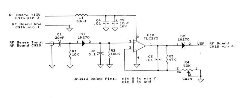
The ALC circuit designed by WA3U as described in Cheesebits August 1996.
The circuit samples a small amount of RF from the transverter out jack through C1. It is converted to a DC voltage by D1 and C2. U1 amplifies this voltage with gain set by R4. D2 is used to isolate the output of U1 so it can be placed in parallel with existing circuitry. No switching is required as the rig is moved from HF to transverter operation. The circuit can be build on a small piece of perf-board and mounted inside the rig between the RF and IF boards. A short length of RG-174 coax was soldered on the bottom of RF board CN25 to sample the transverter out signal. Connections to CN16 were made by sticking the wires next to the wires in the connector. To set R4 for proper gain first disable the transverter output and transmit on 28MHz FM into a dummy load. Adjust the carrier level control so that the ALC reading is half scale. then, enable the transverter output and adjust R4 so that the ALC meter reading is again half scale when transmitting. Do NOT adjust the carrier level in-between.
Note : PE1OGF had to change C2 from 100nf to 10pf !!!! if your ALC is very slow change C2 from 100nf to 10pf.
A hidden menu, not described in the manual can be accessed by pressing the SCAN & TX-M.CH keys while powering ON.
Select with M.CH knob. Set value with up/down buttons, same as normal menu.
Menu 00: Indicates checksum of rom
Menu 01: Turns ON/OFF filter exchange at transmission
Menu 02: Forced ON/OFF AT power down
Menu 03: AT non-stop mode ON/OFF
Menu 04: MODE, FILTER of band memory ON/OFF
Menu 05: Turns ON/OFF a CW greeting message at power ON.
Menu 06: Turns ON/OFF LCD full-On mode at power ON.
Menu 07: Turns ON/OFF DDS subtone
Menu 08: No description - default is OFF
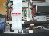
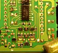
The TS850 noise blanker is not very efficient. A comparison with the diagram of the TS940 circuit, which is very good, shows that the schematics are quite similar except the output of the noise pulse detector. There are 2 bypassing capacitors which are not present in the TS940 schematic. So, the only modification to do is to remove this 10nF capacitors on the NB unit.
The NB board reference is X59-1100-00 and it is located on the upper part of the transceiver at the left of the PA cooling fan.
Remove the upper part of the cabinet and unplug the loud speaker.
You will have to remove 4 screws and unplug 3 connectors in order to extract the board.
The picture at the left shows the board in its normal operating position. (click to enlarge)
The capacitors to remove are C618 and C619. These capacitors are quite small SMD components and hard to locate if you don't have the service manual. In this manual, diagram and board view can be found in the RF unit section.
You should take care when unsoldering the capacitor, they are glued to the board and you should push them gently while heating both ends.
After this modification, the TS850 noise blanker is much more efficient and helps a lot in wipping out electrical QRM. No deterioration has been noticed after this mod.
Gas discharge tube replacement
In order to protect the TS850 against static discharges, Kenwood added a gas discharge tube ref DSA301LA. It is installed on a small PCB just behind the SO239 antenna socket.
With time and discharge process, this tube is leaking and not efficient anymore. This can be detected while looking at the glas enveloppe which has white traces inside the enveloppe. I replaced mine with a ceramic enveloppe discharger which has the same characteristics but does not leak like the original one.
I bought the BOURNS 2049-13 model which can be easily found. Farnell sells it for 0,39 € ex.taxes, which has to be compared with the ridiculous 15-20 € asked by certain "HAM fellows" for this replacement !!
The datasheet can be found here.


