Wintest + skimmer with Perseus SDR
- Details
- Hits: 15499
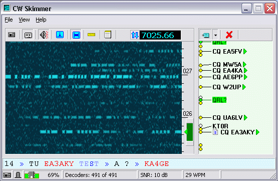 |
How to use Wintest and CW skimmer together ? Configuration used :
|
Monte Renosu - TK/TK-008
- Details
- Hits: 3262
Monte Renosu - TK/TK-008
WWlocator : JN42nb64
Altitude : 2352 m - gain altitude 1150 m - distance 15km A/R
33 QSO 40/10m CW 6 S2S


Capu di u Vitullu - TK/TK-063
- Details
- Hits: 4149
Capu di u Vitullu - TK/TK-063
WWlocator : JN42if34
Altitude : 1331 m - altitude gain +850m
34 QSO 40/30/10m CW 4 US stations


Capu d'Ortu TK/TK-074
- Details
- Hits: 3313
Capu d'Oru TK/TK-074
WWlocator : JN42if48
Altitude : 1294 m
41 QSO 40/20CW - 1 S2S


GPSDO software
- Details
- Hits: 3929
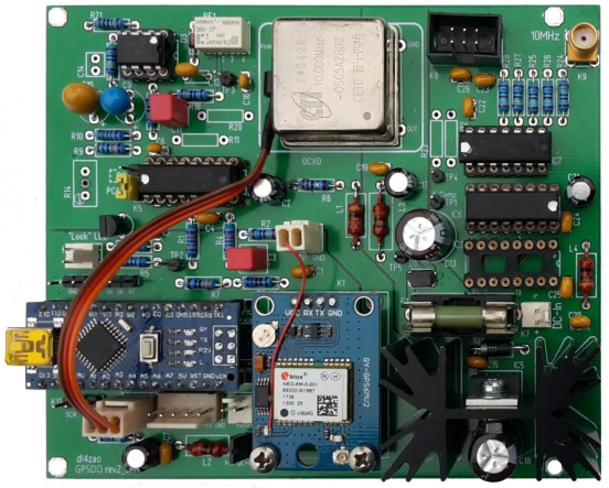
My previous 10 MHz frequency reference having broken down, the question was whether to repair it or move on.
After reflection, I decided to equip myself with a 10 MHz reference disciplined by GPS (GPSDO) in order to obtain the best possible accuracy.
After some research on the Internet, I found ready-made products at affordable prices and some descriptions of amateur achievements.
I chose the option of making the version proposed by DL4ZAO / DL7UKM . On one hand because there is a detailed description (in German) and that the author offered the printed circuit at a correct price, and on the other hand to learn according to the formula " Build and learn ".
The assembly revolves around an Arduino Nano and software is offered by Michael DL7UKM. All the more reason for my choice, now having a good knowledge of this platform.
Page 4 of 7